Become a leader in the IoT community!
Join our community of embedded and IoT practitioners to contribute experience, learn new skills and collaborate with other developers with complementary skillsets.


Join our community of embedded and IoT practitioners to contribute experience, learn new skills and collaborate with other developers with complementary skillsets.


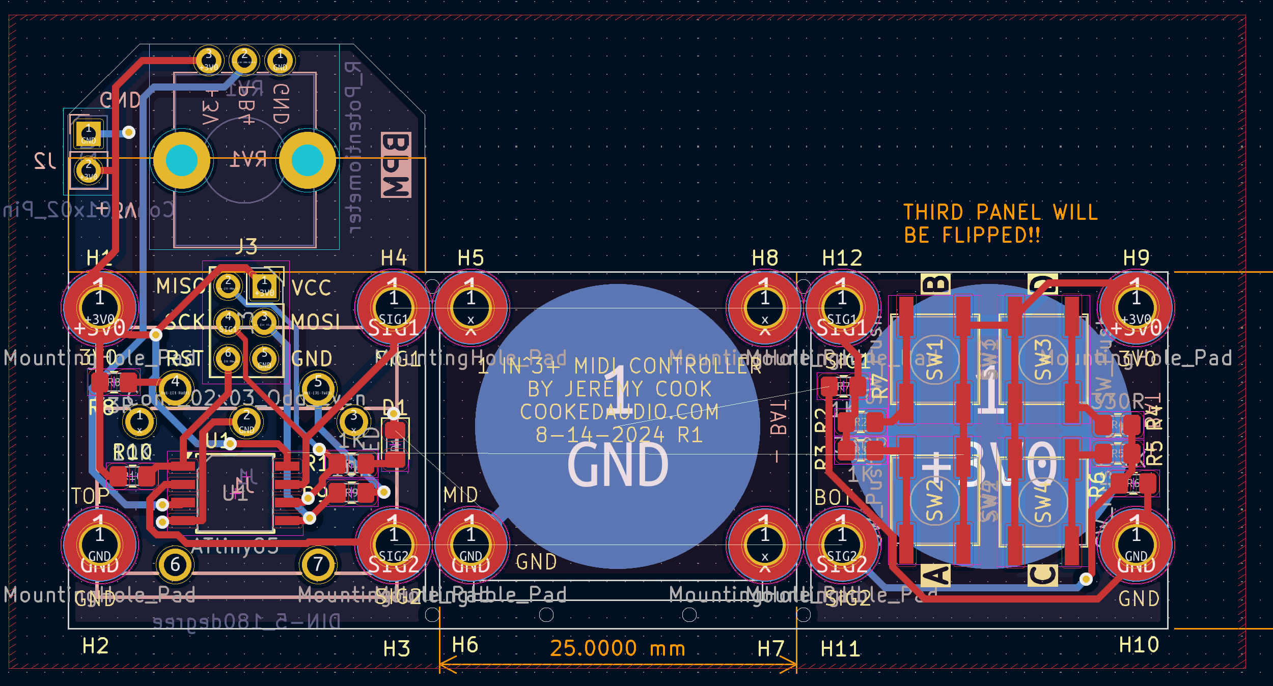
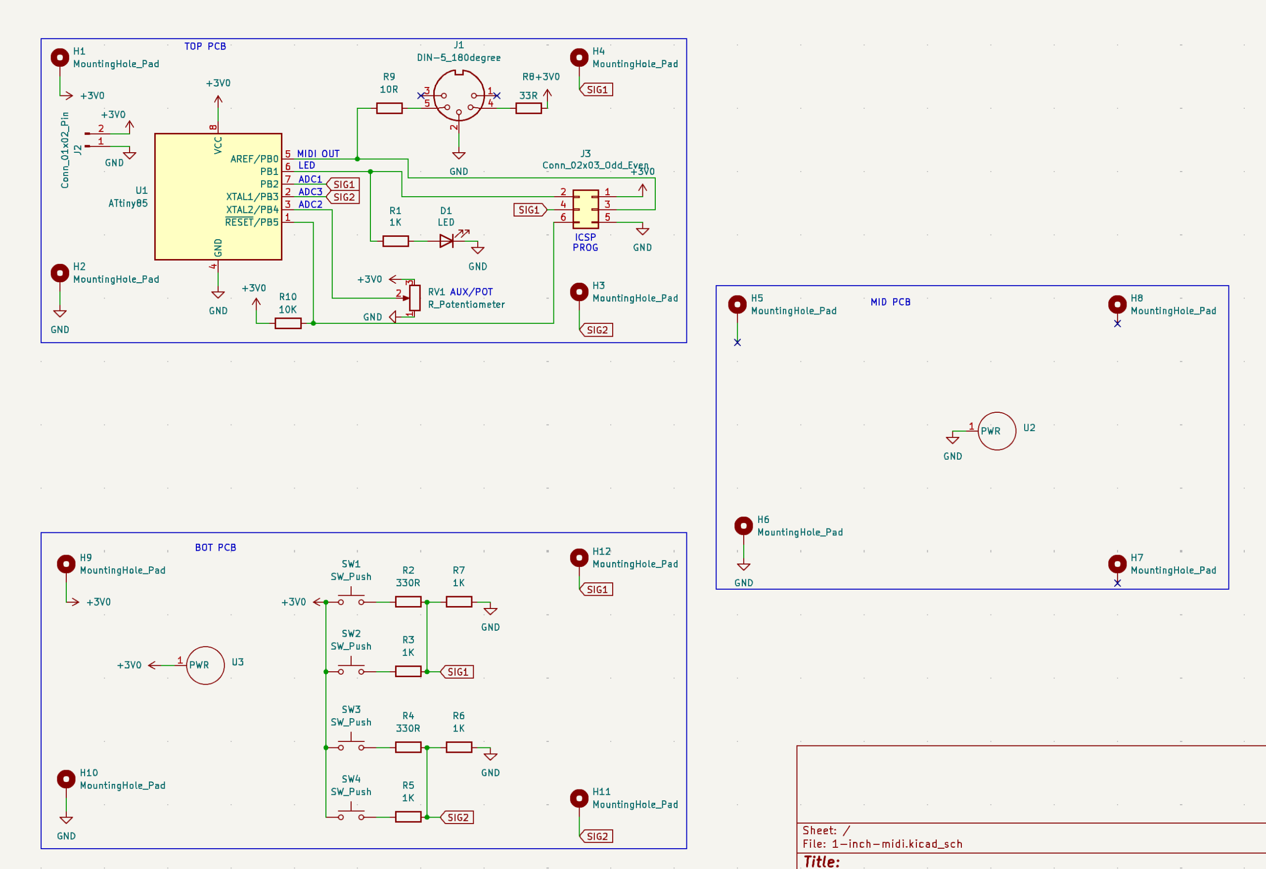
Hi, I’ve got a KiCad project (revised 1-inch-midi) that I’ve been working on that involves 3 boards separated by rat bites. Ground, VCC and two signal pins are passed between the boards via conductive screws nuts. While I think I have a functional design, the error checking function on the PCB editor shows disconnections between these pads as they are not connected as-drawn. Is there a way to put connections into the schematic layout so that the PCB editor is satisfied?
I think it will work as-is, but would be interested in any ideas/suggestions. Also I’m certainly open to any critique of the design in general, as I’m planning to order it soon. I put up an earlier version of the board here for your perusal: https://github.com/JeremySCook/PCBs/tree/main/1-inch-MIDI


I suggest you connect the remaining pads to ground instead of leaving it floating
Perhaps I was not clear. The pads will not be floating, they will be connected via screws that goes from board to board. However, this is not represented properly in the PCB editor so I wonder if there is a way to do so.
Well, leaving it that way won’t have effect on your board. Except you have any other view
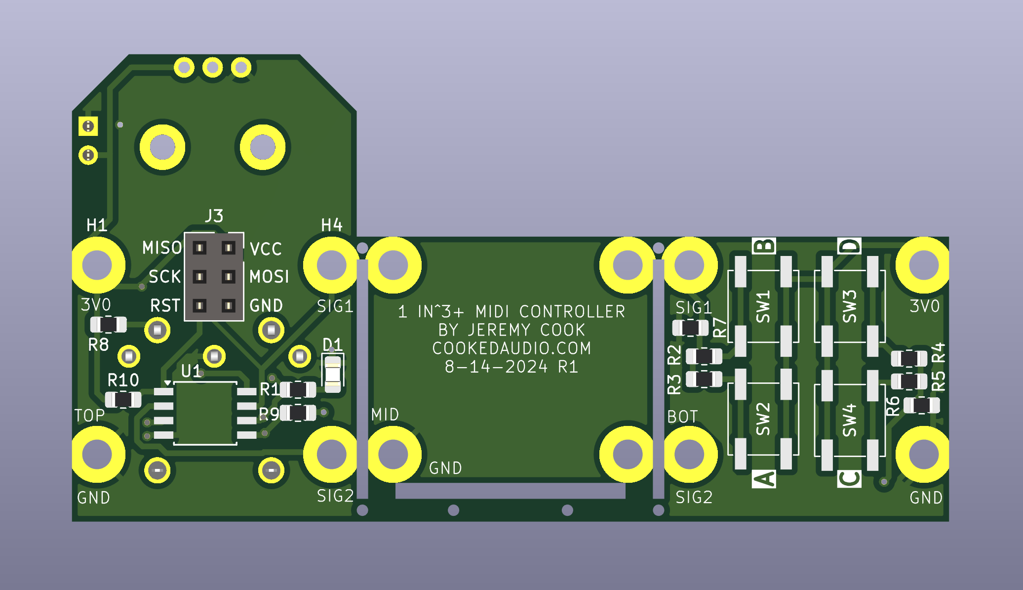
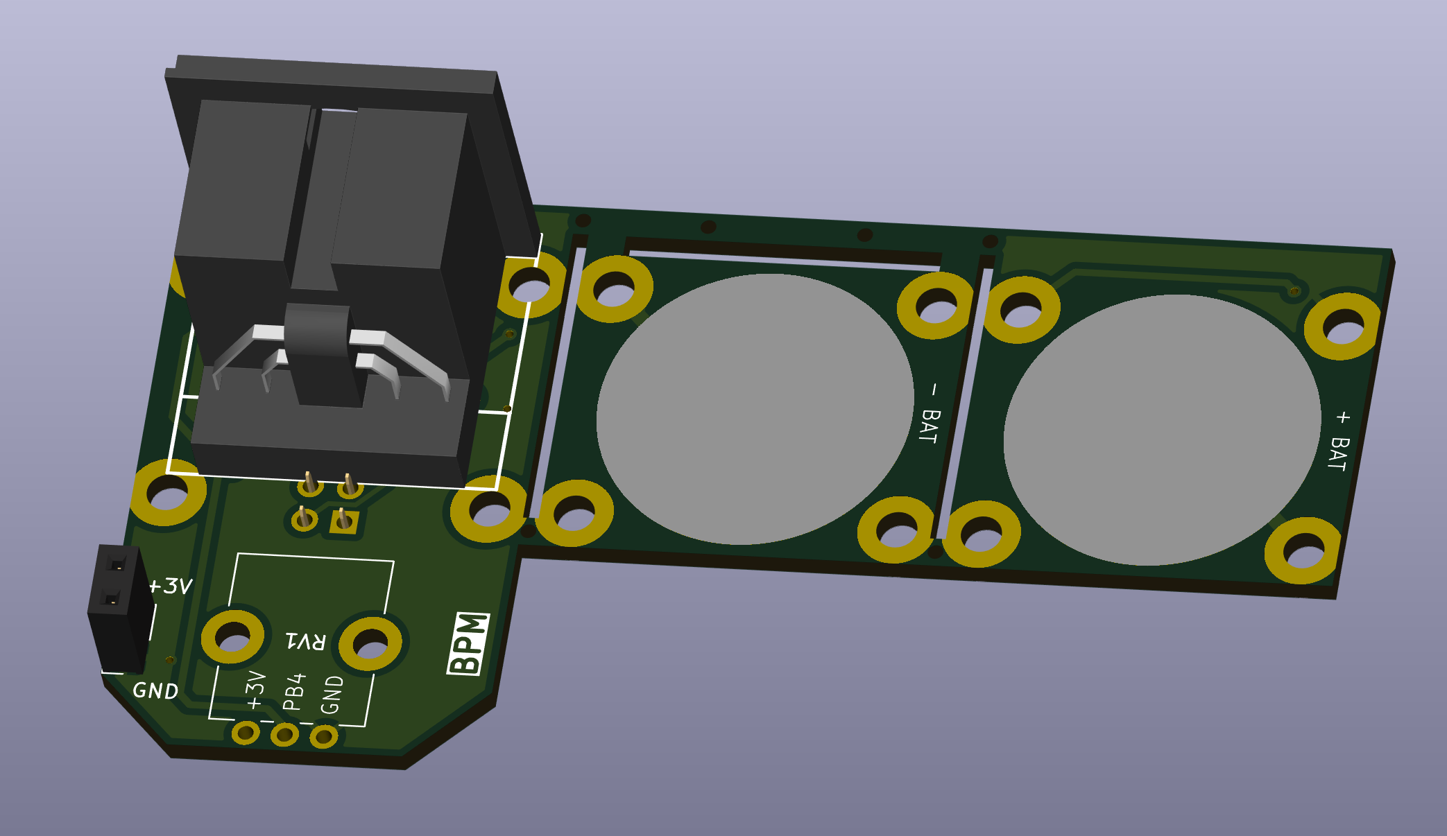
Here are a couple of other views if that is what you mean. Will be stacked up in a similar manner to the third image, but that is an earlier version.
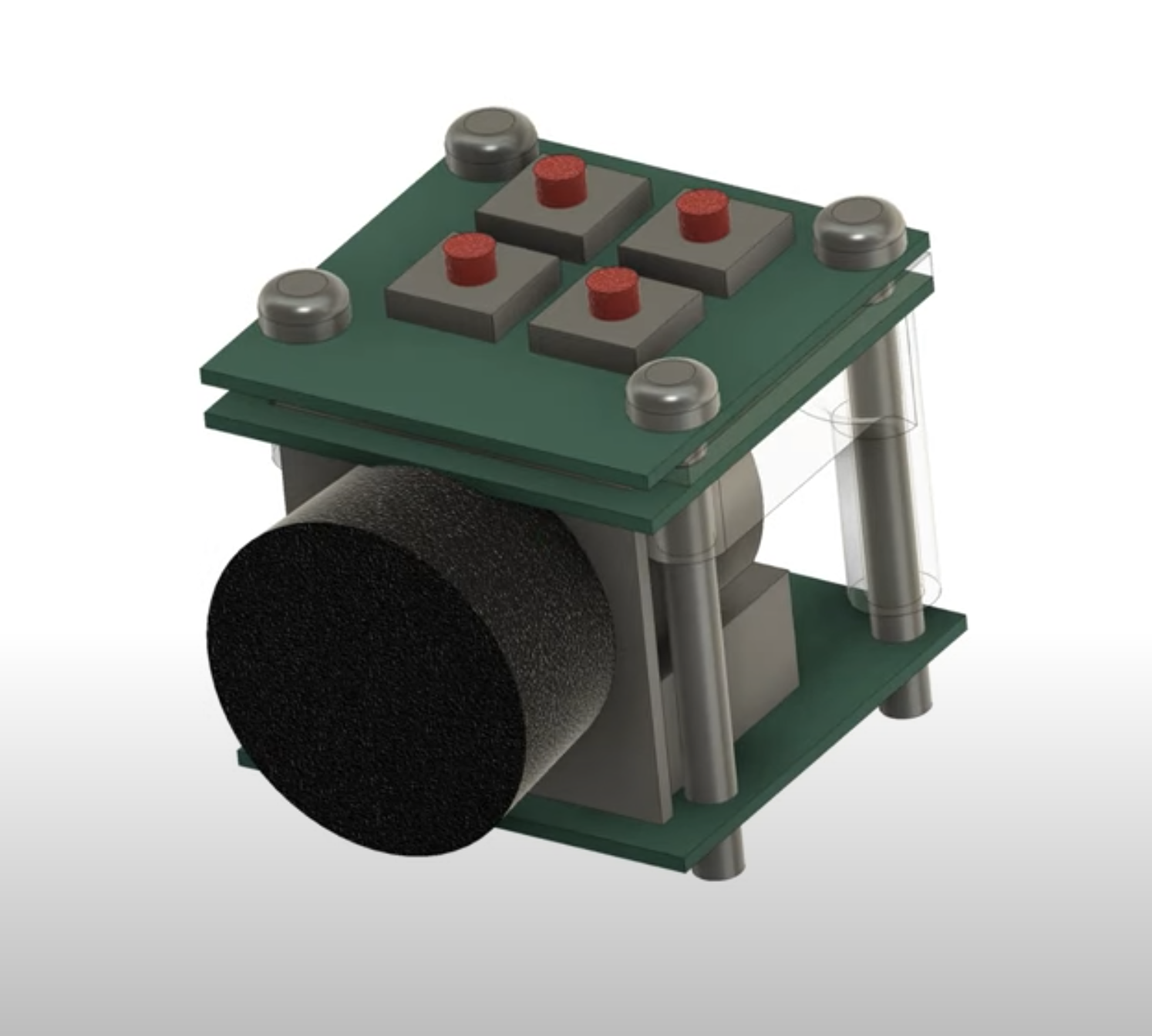
Oo, great design. Well, I haven’t seen a way to do that in kicad for now.
Oo, great design. Well, I haven’t seen a way to do that in kicad for now.
Thanks! Put up the whole explanation of rev 0 here: https://www.youtube.com/watch?v=5Ws_JfCw5NY – planning to add a potentiometer to rev 1!
CONTRIBUTE TO THIS THREAD